Photonics & Optoelectronics
Applications:
- Quantum wells and superlattices.
- Quantum dot and quantum dash active regions.
- Distributed Bragg reflector (DBR) mirror stacks.
- Strain‑engineered heterostructures.
Photonic Integrated Circuits (PIC)
- High‑index‑contrast waveguide multilayers.
- Low‑loss dielectric stacks for routing and confinement.
- Epitaxial III‑V‑on‑Si active regions (UHV‑bonded / UHV‑grown)
- Ferroelectric BTO (BaTiO₃) thin‑film structures for ultrahigh electro‑optic modulation.
- Hybrid BTO–Si and BTO–SiN integration for high‑speed PIC platforms.
Advanced Photovoltaic Structures
Multilayer architectures designed for high‑efficiency light absorption and charge transport.
- Multijunction epitaxial solar cell stacks.
- Graded buffer layers for lattice matching.
- Ultra‑thin tunneling junctions.
- Nanoscale passivation and transport layers.


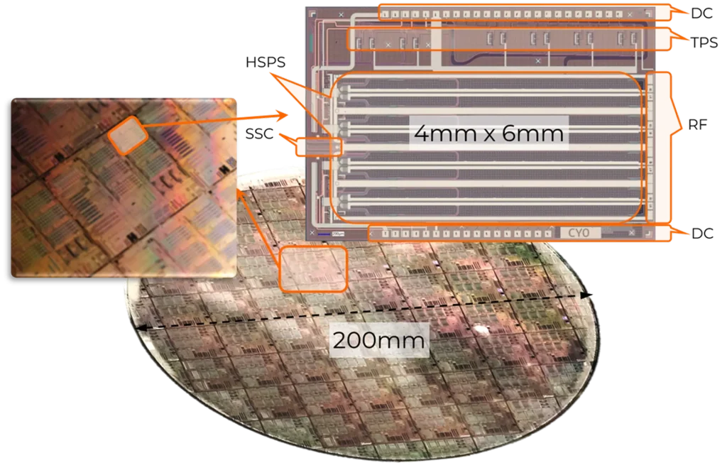
A fully processed 200 mm wafer (BTO on silicon photonics, wafer-level monolithically integrated) showing a zoom-in of a single reticle, and a die shot of a C-band dual-polarization IQ modulator, for up to 130GBd DP-16QAM modulation integrated in a 4×6 mm2 die.
Data Courtesy of Lumiphase AG, Switzerland.
Related Products:
MBE is the primary tool for advanced photonics R&D and production. It is essential for the following:
- Lasers: MBE is used for growing complex quantum cascade laser (QCL) and VCSEL structures requiring ultra-precise layer thickness and composition.
- IR Detectors: MBE grown epitaxial wafers are the “only technology giving the necessary precision” for high-acuity MCT detectors. MBE is also used for QWIPs and antimonide structures.
- MicroLEDs: It enables the incorporation of high indium (In) fractions in GaN to cover the full visible spectrum without phosphorus.
(UHV) Sputtering is crucial for device passivation (protecting laser facets, LED surfaces), depositing dielectric mirrors for VCSELs, and creating transparent conductive oxides (e.g. for displays).


Publications / Results:
- Lumiphase: design and manufacturer of BTO-enhanced SiPh PICs based on their proprietary technology to deliver leading-edge integration, efficiency and scalability to customers worldwide
- Lumiphase: Large Pockels effect in micro- and nanostructured barium titanate integrated on silicon
- LaLuceCristallina: Ultra-compact electro-optical modulators based on monolithic BaTiO3 on silicon
- Applied Optoelectronics, Inc (AOI)
- Optica: OFC 2026 Conference Proceedings
Some images used on this website are sourced from Freepik, FreeImages, Pikwizard, and Unsplash+. We thank the creators and platforms for providing these resources.