
12″ (300mm) Barium Titanate (BTO)
Barium Titanate (BTO) on 12" (300 mm) Silicon. Proven performance for next-generation photonics.
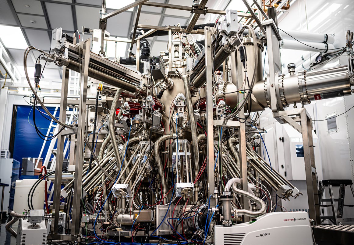
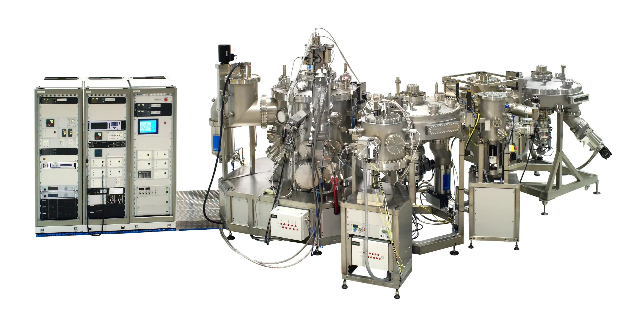
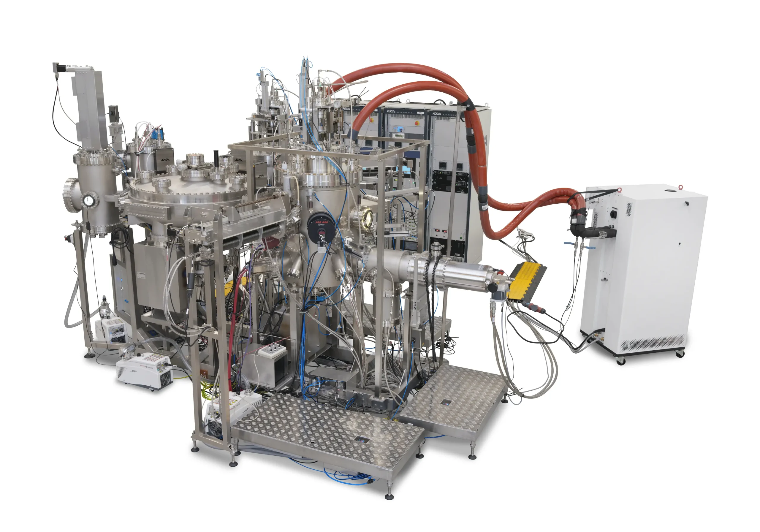
Production oxide MBE from DCA Instruments makes BTO-on-silicon photonics manufacturable – FOUP-to-FOUP automation, consistent results wafer after wafer, and high-quality epitaxial BTO on a proven, reliable platform.
Key messages:
- BTO is the modulator material AI interconnects need
- Automated: a fab tool, not a lab tool
- Productive: delivering output, wafer after wafer
- Proven results
- In production flows today
Key features:
- 24/7 batch processing, ultra-low-particle, SEMI-FAB-compliant
- Automated FOUP loading, wafer ID recognition and flipping
- UHV transfer and wafer tracking by the CDC robot
- 8″ (200mm) or 12″ (300mm) wafer size
- Surface prep and MBE growth with closed-loop feedback, with real-time flux and growth manipulation using integrated RHEED and XBS
- MOSAIC Software


Why BTO? A strong Pockels material made for silicon
- Fully CMOS compatible: epitaxial BTO on Si via an MBE-grown SrTiO<sub>3</sub> seed; integration steps commonly available in CMOS back-end-of-line processing; monolithically integrated in a 300 mm SiPh foundry process with 95 % functional yield. [Abel, Nat. Mater. 2019; PsiQuantum, Nature 2025]
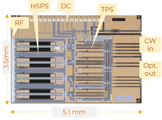
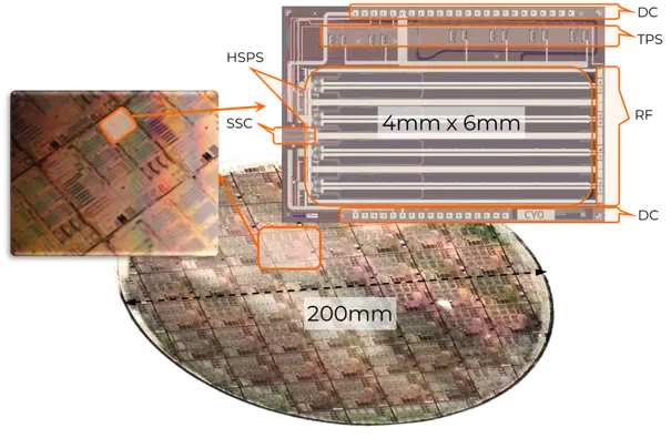
- High Pockels effect (~923 pm/V, one of the largest on silicon) → smaller modulators, denser arrays: 1.75 mm phase shifters reach 105 GHz; four modulators on a 5.1 × 3.5 mm² die; 350 µm phase shifters for a full π shift in a 116-actuator mesh. [OFC 2026; Nat. Photon. 2026]
- Field-driven, low power: no carrier injection; bias held at < 5 mW vs 13 mW per thermal phase shift; 560 nW per π static power, no thermal crosstalk. [OFC 2026; Nat. Photon. 2026]
BTO beyond datacom
- Non-volatile photonic memory: ferroelectric domains hold an optical state with no holding power; multilevel non-volatile phase shifters (16 levels shown). [Geler-Kremer, Nat. Photon. 16, 491 (2022); Catalá-Lahoz, Nat. Photon. 20, 932 (2026)]
- Programmable photonics & optical computing: 116-actuator BTO gate array, ~80 ns switching; filters, 4×4 linear transforms, routing. [Nat. Photon. 2026]
- Quantum photonics: low-loss BTO switches for photon routing (0.33 dB·V) [PsiQuantum, Nature 2025]; Pockels effect retained at 4 K (~200 pm/V) [Eltes, Nat. Mat. 19, 1164–1168 (2020)].
- Robust operation: modulation maintained above the bulk Curie point (tested to 130 °C); no degradation after 250 °C exposure; 24 h at 90 °C. [Messner, JLT 37, 281 (2019)]
The enabling step: an MBE-grown SrTiO3 (STO) template layer
- Without an MBE-grown SrTiO3 seed layer, high-quality epitaxial BTO films on silicon cannot be achieved.
- The few-atomic-layer seed locks into registry with silicon and templates single-crystal BTO; sputtered and hybrid-MBE BTO also build on it.
Automated: a fab tool, not a lab tool:
- In 2019 DCA built the world’s first production oxide MBE for 300 mm wafers.
- Wafers go in and come out in FOUPs. The EFEM has dual FOUP ports, the load lock and storage hold 10 or 25 wafers, and a robot moves wafers under ultra-high vacuum.
- Software runs the whole process: wafer ID and tracking, growth recipes with closed-loop feedback, safety interlocks, 24/7 batch processing and SECS/GEM connection to the factory system.
- Production proven Automated Transfer Robot validated for over 25,000 transfer cycles, delivers long-term operational robustness and repeatability.
- Wafer temperature uniformity of ±2.0 °C at 600 °C for precise, repeatable BTO growth.
Every BTO route on one flexible, fully automated DCA platform
- Solid-source MBE – Ti from DCA HTEC high-temperature effusion cell or e-beam evaporator: highest controllability, excellent material quality.
- Hybrid MBE – Ti from DCA MOPI metal-organic injector: faster growth; Vπ and propagation loss comparable to other growth methods.
- UHV sputtering – DCA APEX-L linear magnetron for 8″–12″: simpler processing, higher throughput, on the MBE seed.
- DCA MOSAIC software: automated flux calibration and closed-loop source control for optimal stoichiometry; parallel layer-based recipes; SECS/GEM.
Delivering output
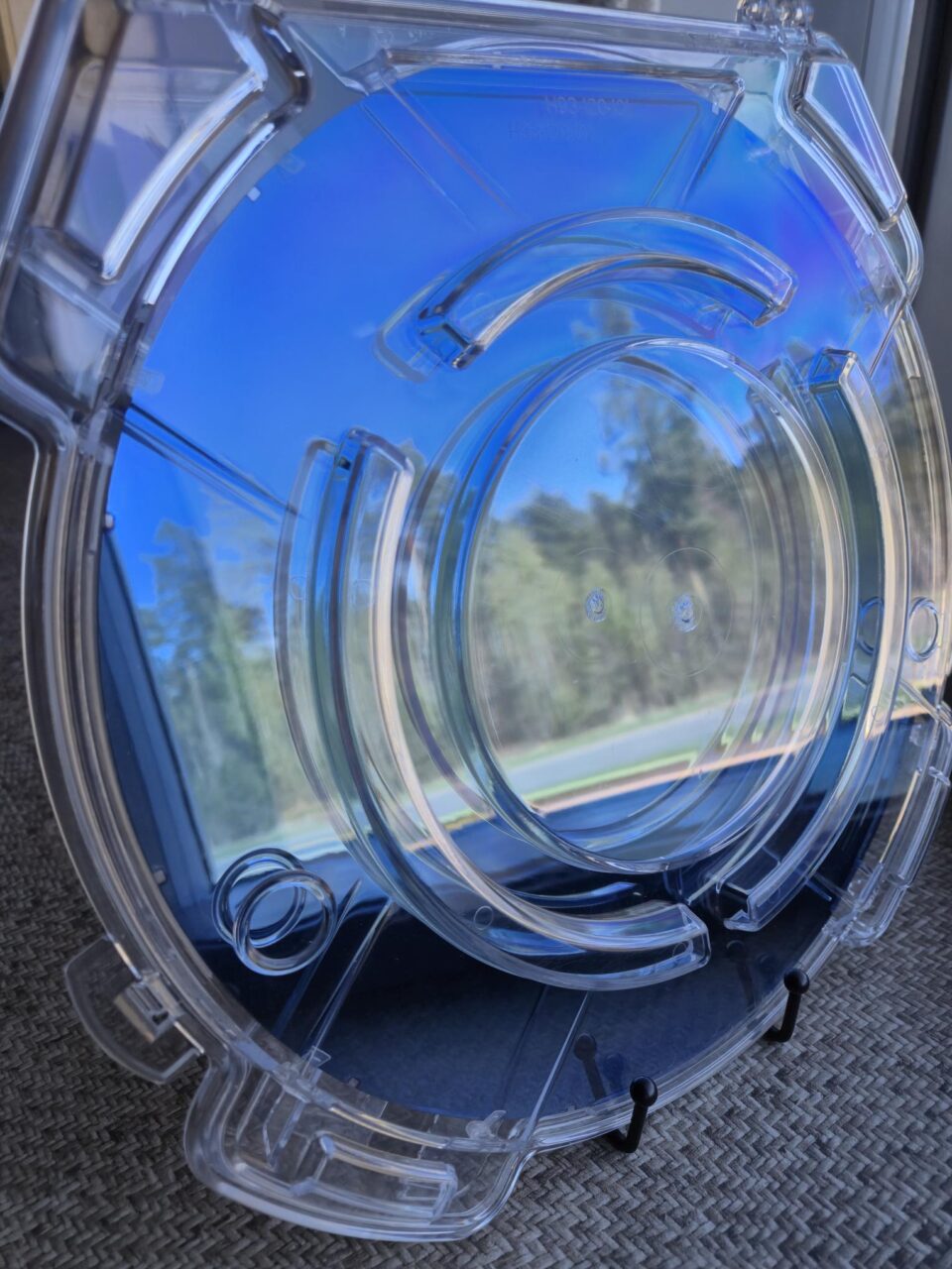
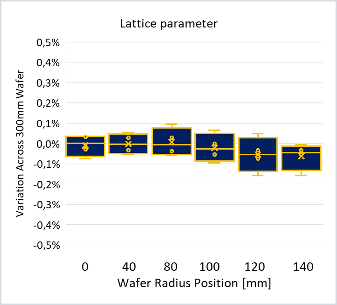
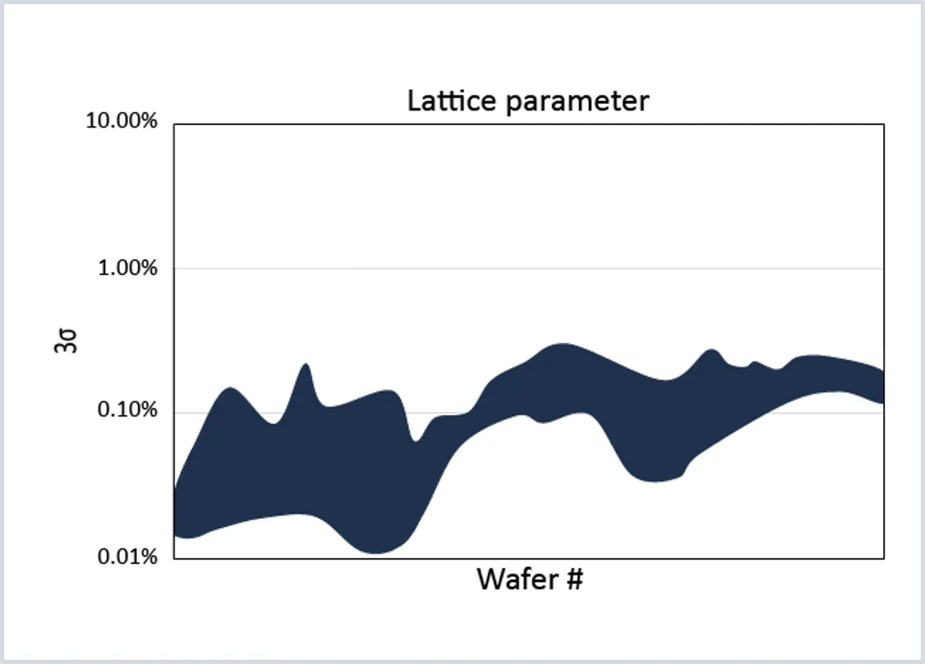
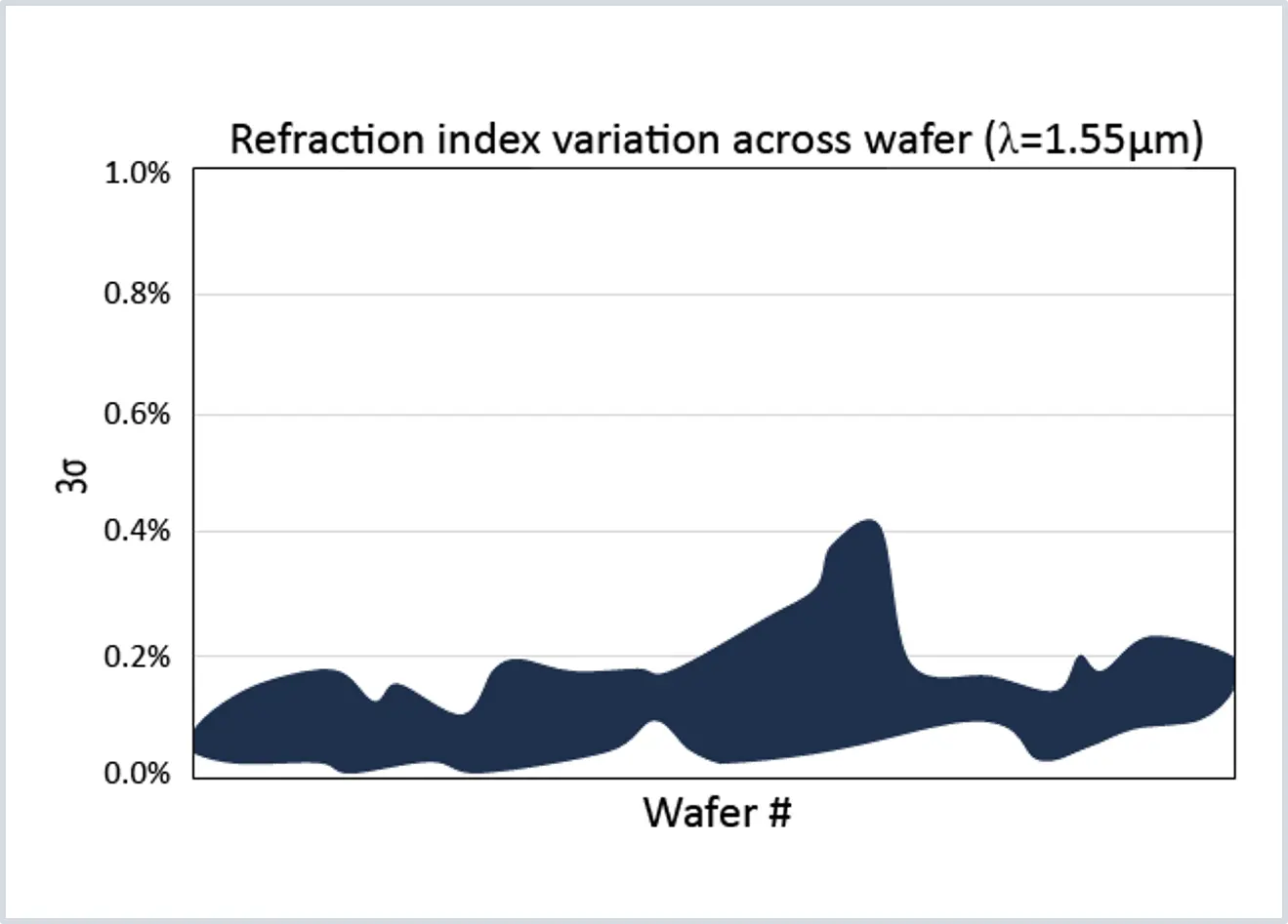
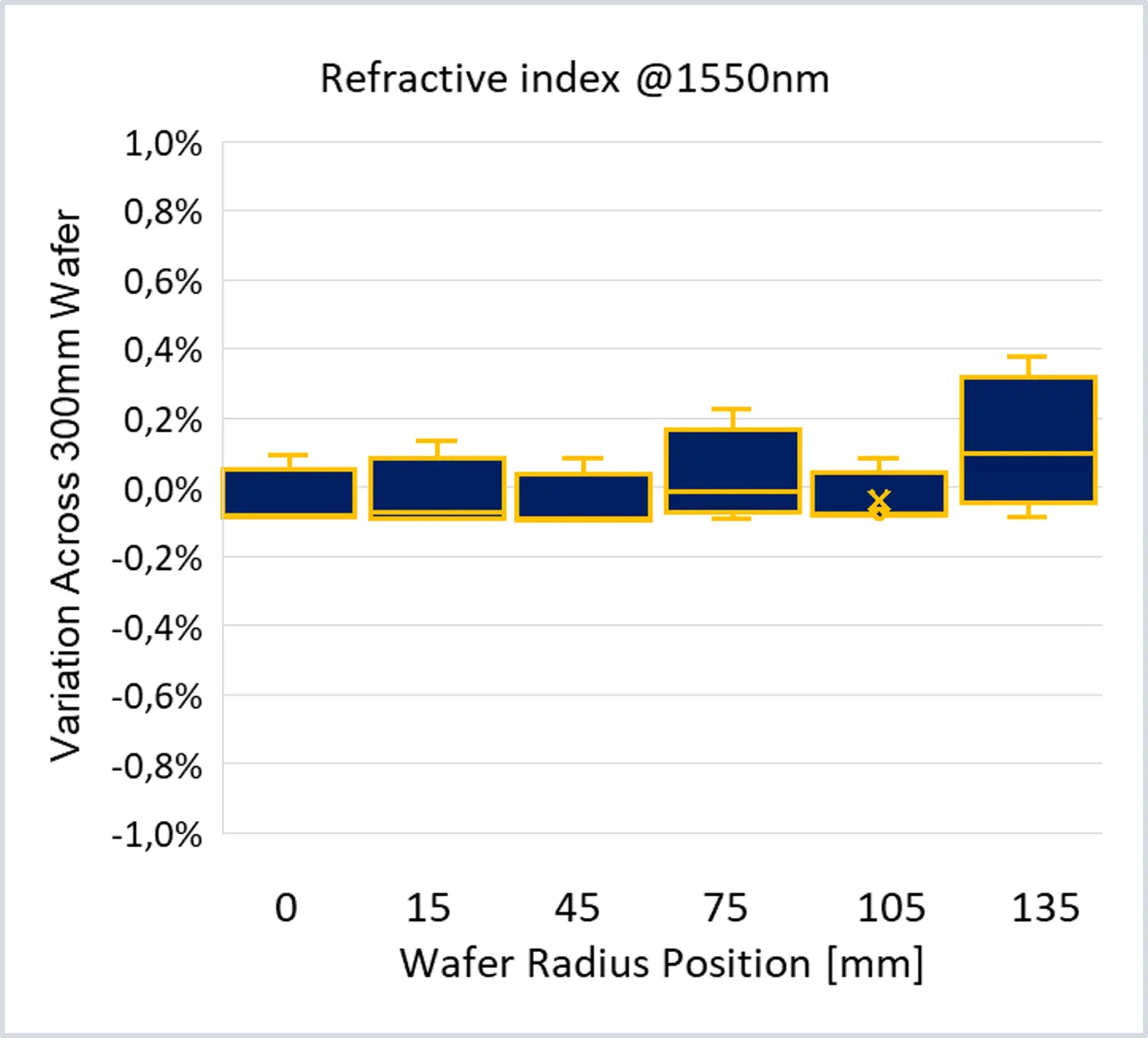
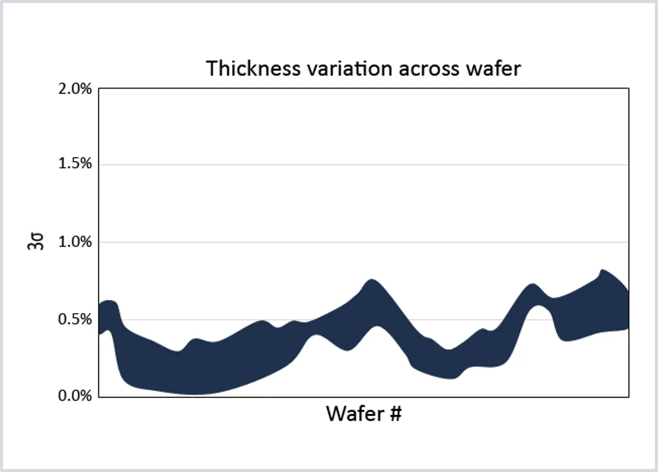
- 100 BTO wafers on 300 mm, with 3σ variation:
- lattice parameter about 0.1 %
- thickness under 1 %
- refractive index typically under 0.2 %
- Uniform centre to edge: lattice within ±0.2 %, refractive index within ±0.4 % across the 300 mm wafer.
- 12″ wafers double device throughput vs 8″.
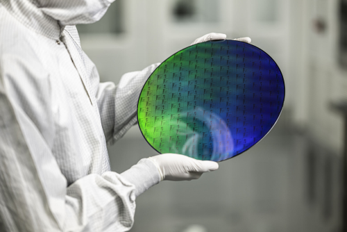
- Visuals: 3σ graphs; “Lattice parameter_300mm_DCA” and “Refractive index_300mm_DCA”; 300 mm BTO wafer photo.
Proven results
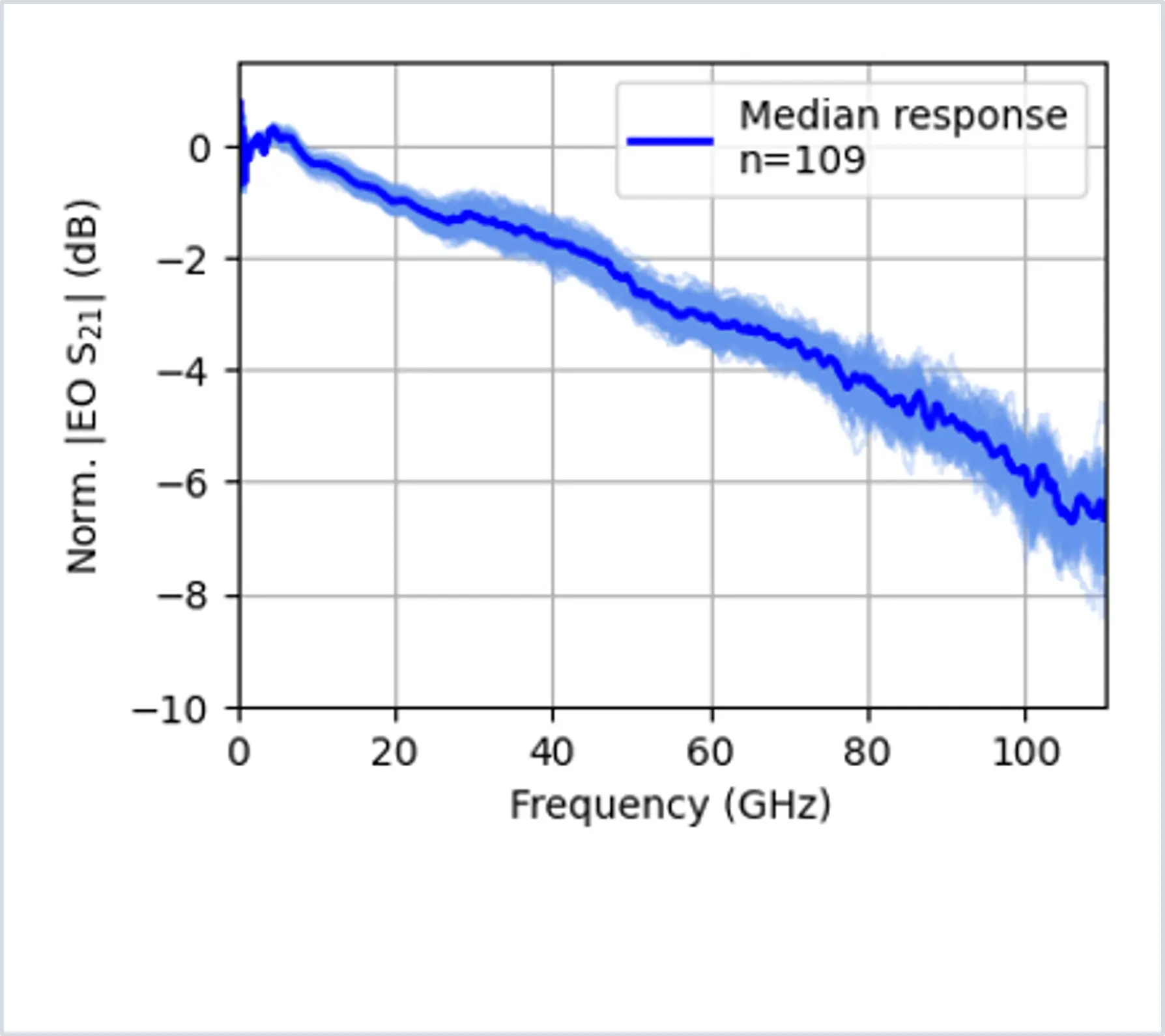
- OFC 2026 (McGill, Ciena, Lumiphase): net 1.6 Tb/s (4 × 448 Gb/s PAM4, 2 km), 105 GHz, consistent 20–85 °C, on epitaxial BTO grown on DCA metal-oxide MBE systems; companion DP-IQ modulator: net 1 Tb/s per wavelength [Link].
Trusted by Industry Leaders:
- Lumiphase (Switzerland) – Device maker: manufactures BTO-enhanced SiPh PICs based on proprietary technology to deliver leading-edge integration, efficiency and scalability to customers worldwide. MBE-grown BTO in 200 and 300 mm SiPh flows.
- PsiQuantum (USA) – Photonic quantum computing: manufactures photonic components, including single photon sources, single-photon detectors, and an ultra-high-performance optical switches for photonic quantum computing. Photonic quantum computing, 300 mm foundry flow.
- La Luce Cristallina (USA) – Manufacturer of STO/BTO wafers: manufactures epitaxial BTO and STO wafer platforms integrated with silicon and silicon-on-insulator (SOI). Available across multiple wafer sizes, orientations, and material thicknesses, supporting the development of next-generation photonic, sensing, quantum, and semiconductor devices.
Three business models, one enabling step: precision epitaxy on production-grade DCA tools.
Video credit to PsiQuantum: 300mm-BTO Production Tool (DCA M1000)
Publications/Results:
- Nature: A manufacturable platform for photonic quantum computing
- Nature Materials: Large Pockels effect in BTO
- Nature Materials 2020: An integrated optical modulator operating at cryogenic temperatures
- Nature Photonics: High-speed non-volatile barium titanate field-programmable photonic gate array
- Nature Photonics: A ferroelectric multilevel non-volatile photonic phase shifter
- Optica: Plasmonic Ferroelectric Modulators
- Optica: BTO poling dynamics in High-Speed Communications
- Optica: OFC 2026 Conference Proceedings
