
Proven performance for next-generation photonics.
Production oxide MBE from DCA Instruments makes BTO-on-silicon photonics manufacturable – FOUP-to-FOUP automation, consistent results wafer after wafer, and high-quality epitaxial BTO on a proven, reliable platform.
- 1.6 Tb/snet (4 × 448 Gb/s PAM4) on BTO grown on DCA MBE – OFC 2026 [3]
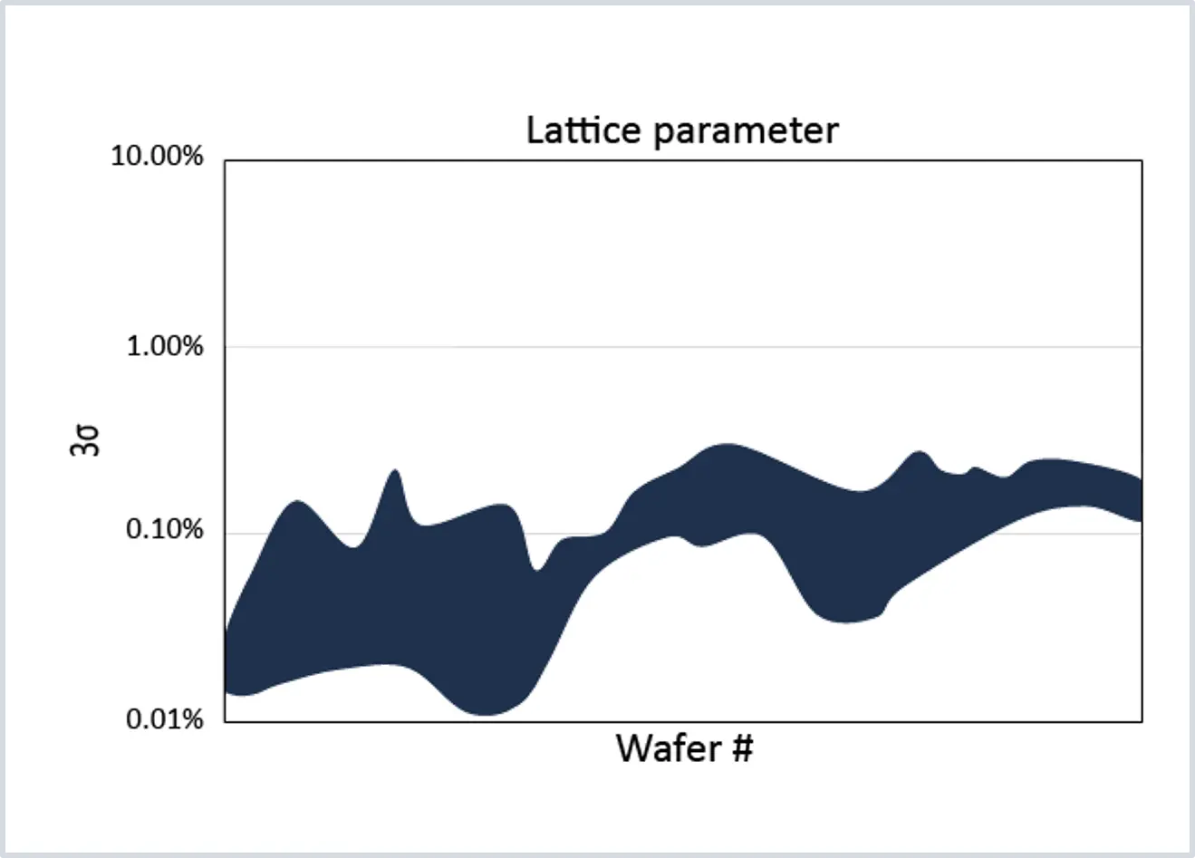
- >100BTO wafers with 3σ lattice-parameter variation ≈ 0.1 %
- 24/7FOUP-to-FOUP batch processing with SECS/GEM factory connection
- 25,000+transfer cycles validated on the automated UHV robot
Why BTO? A strong Pockels material made for silicon
Fully CMOS compatible
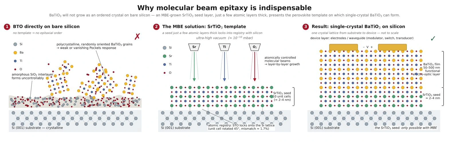
Epitaxial BTO (BaTiO3) grows on silicon via an MBE-grown SrTiO3 (STO) seed. The integration steps are commonly available in CMOS back-end-of-line processing, and BTO has been monolithically integrated in a 300 mm SiPh foundry process with 95 % functional yield. [1, 2]
Smaller, denser modulators
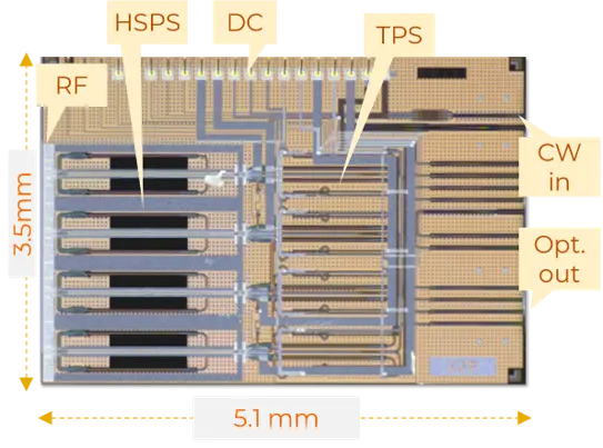
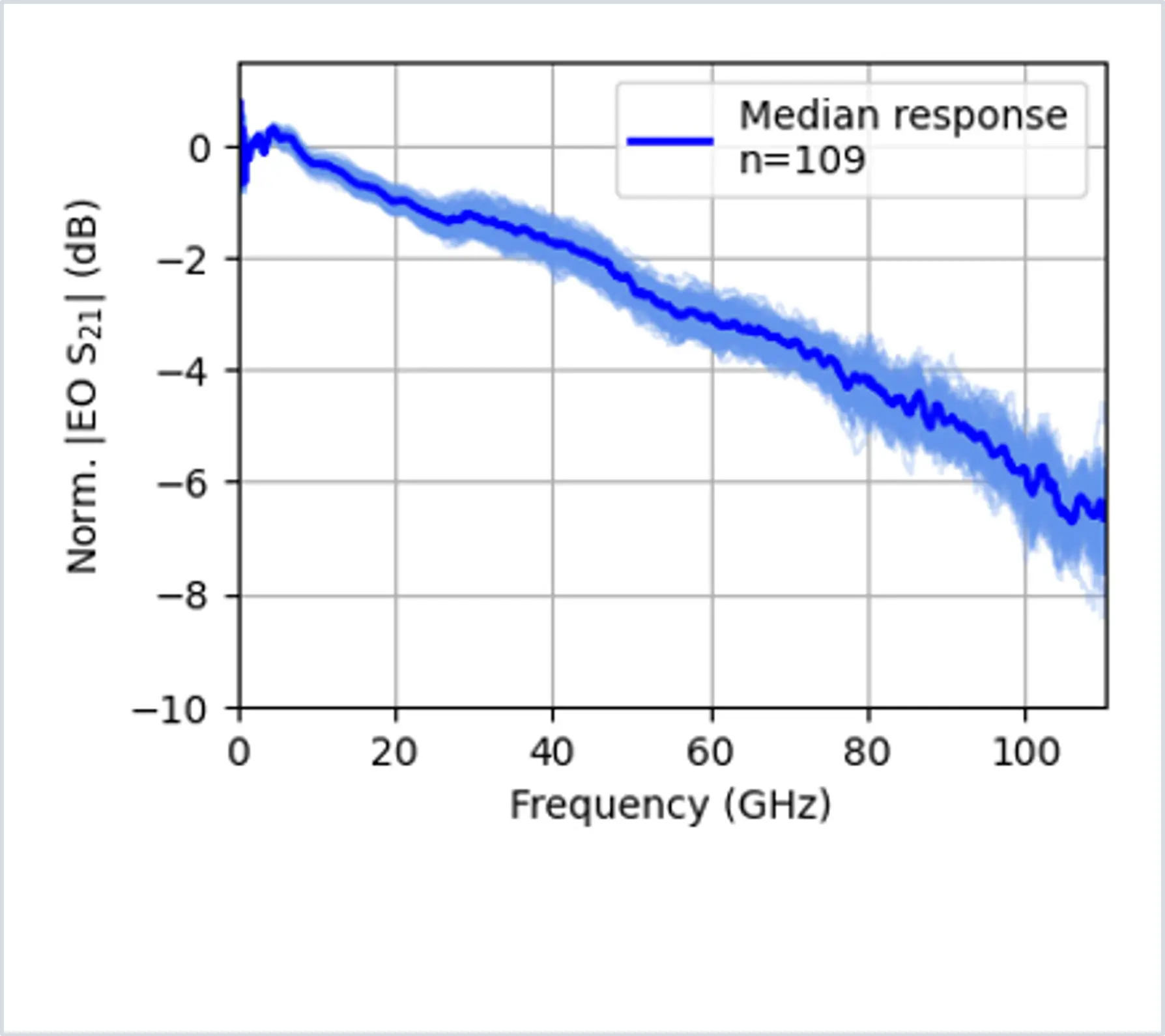
BTO’s Pockels coefficient (~923 pm/V) is one of the largest on silicon: 1.75 mm phase shifters reach 105 GHz, four modulators fit on a 5.1 × 3.5 mm² die, and 350 µm phase shifters give a full π shift in a 116-actuator mesh. [3, 5]
Low power, no heat
BTO is field-driven, with no carrier injection. DC bias tuning stays below 5 mW, against 13 mW per π for a thermal phase shifter. Static power is 560 nW per π, with no thermal crosstalk. [3, 4, 5]

Read why BTO is emerging for integrated photonic platforms
BTO beyond datacom
- Non-volatile photonic memoryFerroelectric domains hold an optical state with no holding power; multilevel non-volatile phase shifters (16 levels shown). [6, 5]
- Programmable photonics and optical computing116-actuator BTO gate array with ~80 ns switching, for filters, 4×4 linear transforms and routing. [5]
- Quantum photonicsLow-loss BTO switches for photon routing (0.33 dB·V) [2]; Pockels effect retained at 4 K (~200 pm/V). [7]
- Robust operationModulation maintained above the bulk Curie point (tested to 130 °C); no degradation after 250 °C exposure; 24 h at 90 °C. [8]
Proven results
At OFC 2026, McGill, Ciena and Lumiphase showed a BTO/silicon-photonics transmitter carrying a net 1.6 Tb/s (4 × 448 Gb/s PAM4 over 2 km) with 105 GHz bandwidth and consistent performance from 20 to 85 °C – built on epitaxial BTO grown on DCA metal-oxide MBE systems. A companion DP-IQ modulator reached a net 1 Tb/s per wavelength. [3, 4]
Productive: delivering output, wafer after wafer
3σ statistics over more than 100 BTO wafers on silicon, grown by solid-source MBE.
- Lattice parameter (indicator of Ba/Ti stoichiometry)
- ≈ 0.1 %3σ variation
- Thickness
- < 1 %3σ variation, films > 150 nm
- Refractive index
- < 0.2 %typical 3σ variation
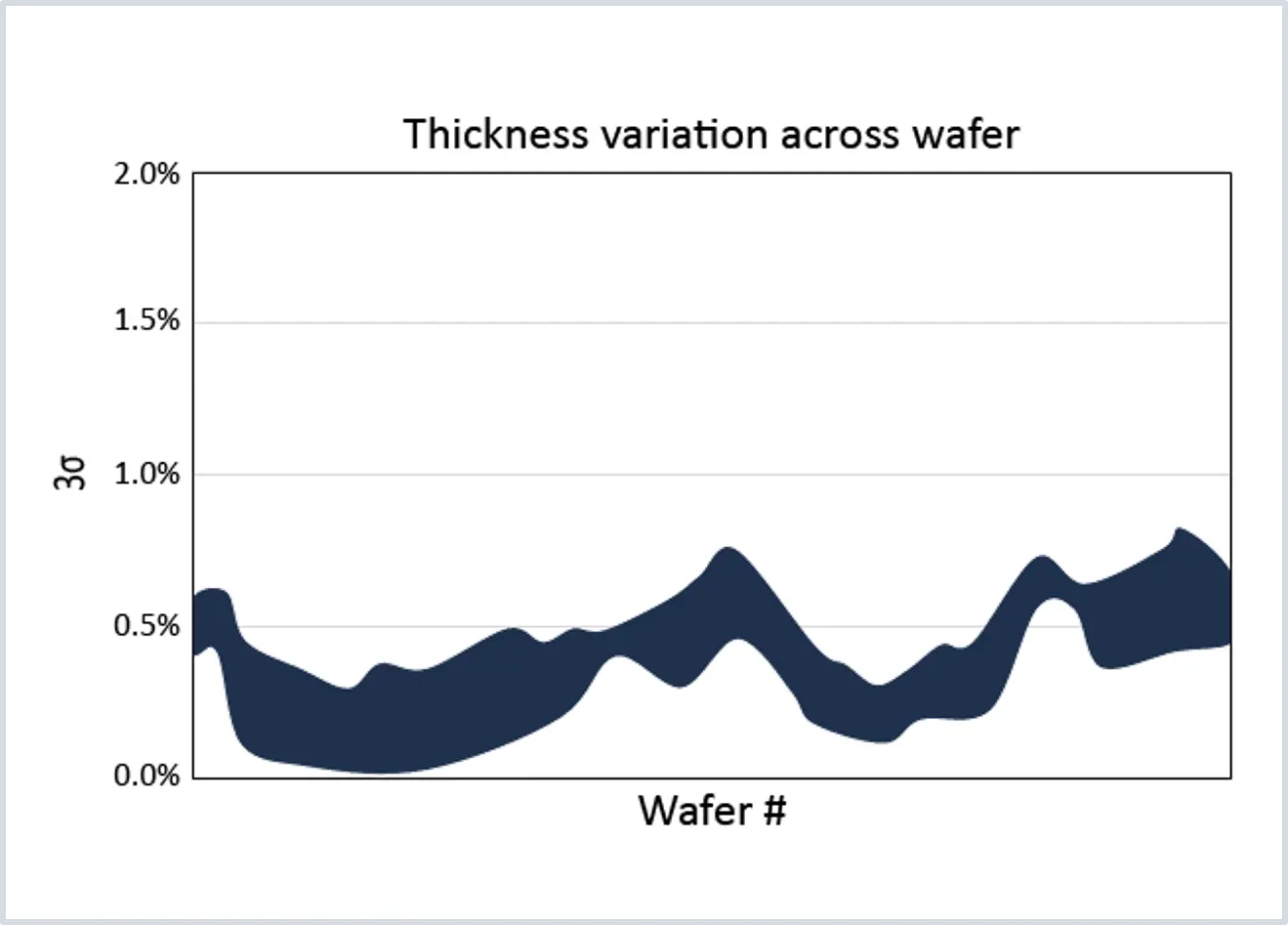
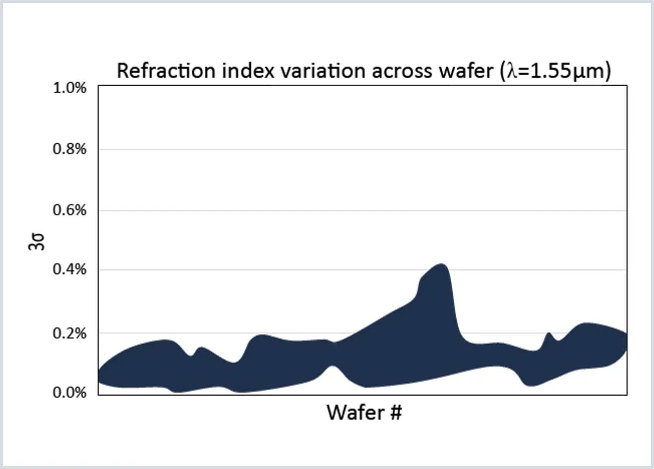
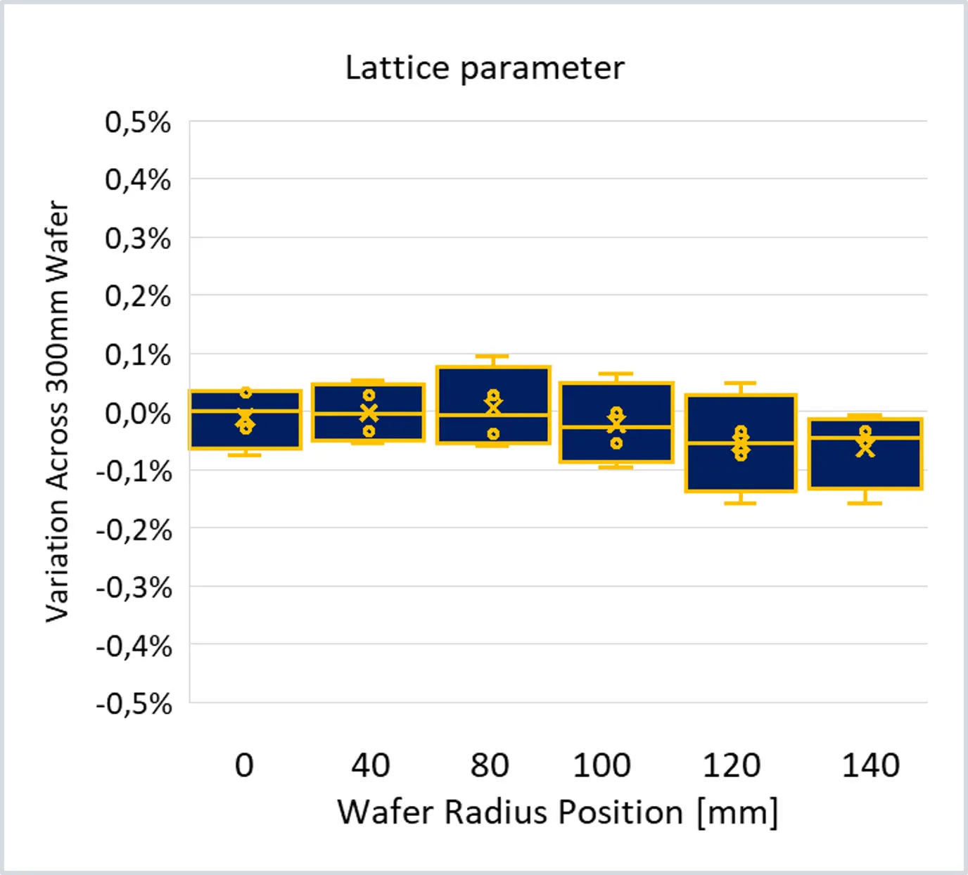
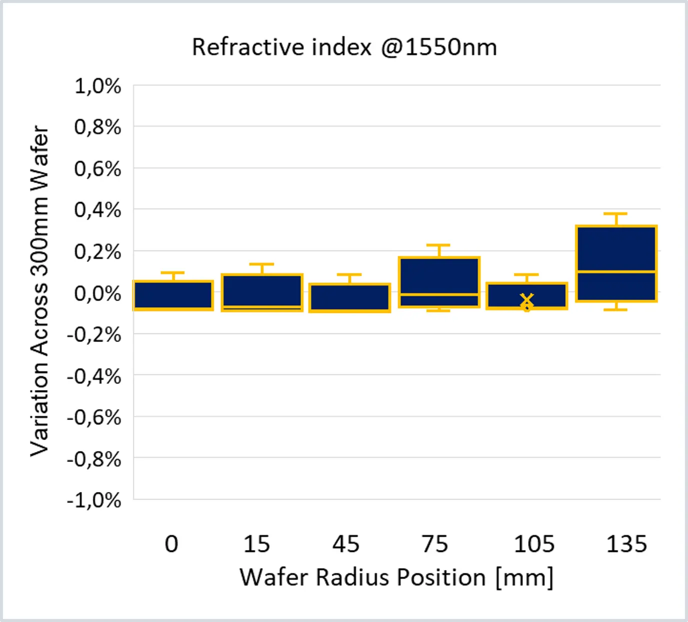
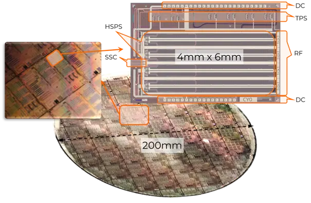
Uniform from centre to edgeLattice parameter within ±0.2 % and refractive index within ±0.4 % across the 300 mm wafer. 300 mm wafers double device throughput compared with 200 mm wafers.
Automated: a fab tool, not a lab tool
In 2019 DCA built the world’s first production oxide MBE for 300 mm wafers. Wafers go in and come out in FOUPs under a fully automated 24/7 batch process.
| Wafer size | 8″ (200 mm) or 12″ (300 mm) |
|---|---|
| Loading | EFEM with dual FOUP ports; wafer ID recognition and flipping |
| Capacity | Load lock and storage for 10 or 25 wafers |
| UHV transfer | Automated transfer robot (CDC), validated for over 25,000 transfer cycles |
| Scalability | One robot serves multiple growth chambers (e.g. dual M1000 MBE); additional CDCs extend the cluster tool to up to four M1000 growth chambers |
| Temperature uniformity | ±2.0 °C at 600 °C for precise, repeatable BTO growth |
| Process control | Surface preparation and MBE growth with closed-loop feedback; real-time flux and growth control with integrated RHEED and XBS |
| Software | DCA MOSAIC runs every BTO route: wafer ID and tracking, automated flux calibration and closed-loop source control for optimal stoichiometry, parallel layer-based growth recipes, safety interlocks, 24/7 batch processing and SECS/GEM |
| Cleanliness | Ultra-low particle, SEMI-FAB compliant. Particle count over a 300 mm Si wafer: 25 after transfer to chambers, 91 after heating to 800 °C with rotation (M-Series data) |

Every BTO route on one flexible, fully automated DCA platform
The enabling step: an MBE-grown SrTiO3 seed
Without an MBE-grown SrTiO3 (STO) seed layer, high-quality epitaxial BTO films on silicon cannot be achieved. The few-atomic-layer seed locks into registry with silicon and templates single-crystal BTO; sputtered and hybrid-MBE BTO also build on it.
| Route | DCA source | Strength |
|---|---|---|
| Solid-source MBE | Ti from DCA HTEC high-temperature effusion cell or e-beam evaporator | Highest controllability, excellent material quality |
| Hybrid MBE | Ti from DCA MOPI metal-organic injector | Faster growth; proven on 200 mm wafers, with Vπ and propagation loss comparable to solid-source MBE |
| UHV sputtering | DCA APEX-L linear magnetron for 8″–12″ | Simpler processing, higher throughput, on the MBE seed |
BTO grown on 200 mm wafers by Hybrid MBE - proven device performance
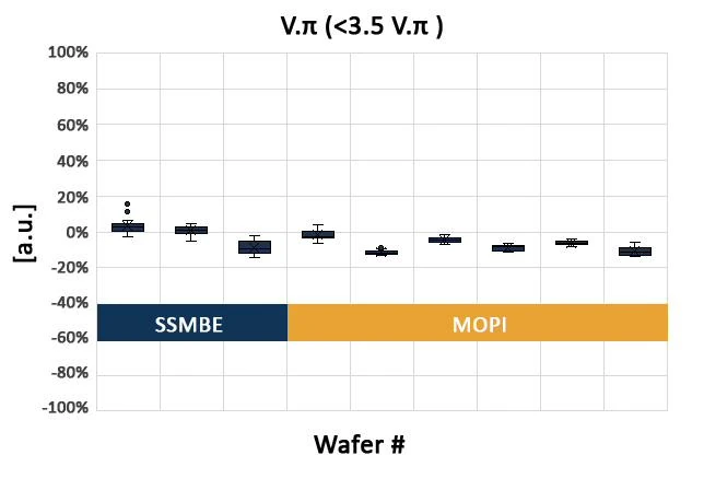
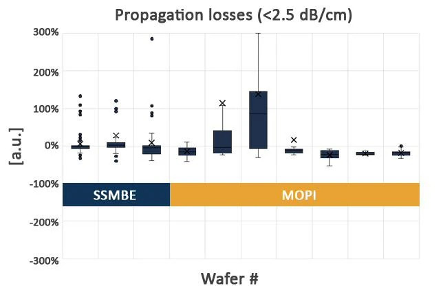
Faster growth, comparable devicesThe MOPI source supplies titanium as a metal-organic precursor, for faster growth and higher throughput. Device Vπ and propagation loss are comparable to solid-source MBE.
In production flows today
Three business models, one enabling step: precision epitaxy on production-grade DCA tools.
Lumiphase
Manufactures BTO-enhanced silicon-photonics PICs based on proprietary technology.
MBE-grown BTO in 200 and 300 mm SiPh flows.
PsiQuantum
Manufactures photonic components, including single-photon sources, single-photon detectors and ultra-high-performance optical switches.
300 mm foundry flow.
La Luce Cristallina
Supplies epitaxial BTO and STO wafer platforms on silicon and SOI, in multiple wafer sizes, orientations and thicknesses.
DCA MBE for the STO seed, DCA UHV sputtering for BTO.

Talk to us about BTO production on 200 / 300 mm
Dr Sabina Hatch, Sales Director – sabina.hatch@dca.fi
References
- S. Abel et al., “Large Pockels effect in micro- and nanostructured barium titanate integrated on silicon”, Nature Materials 18, 42–47 (2019). doi:10.1038/s41563-018-0208-0
- Alexander et al. (PsiQuantum), “A manufacturable platform for photonic quantum computing”, Nature 641, 876–883 (2025). doi:10.1038/s41586-025-08820-7
- B. Qiu et al., “Barium Titanate Enabling Net 1.6T (4×448 Gbps PAM4) On a Silicon Photonics Platform”, OFC 2026, postdeadline paper Th4B.3.
- B. Qiu et al., “Barium Titanate DP-IQM Enabling Net 1 Tbps/λ ZR and Coherent-Lite Data Center Networks”, OFC 2026, paper Th3J.4.
- C. Catalá-Lahoz et al., “High-speed non-volatile barium titanate field-programmable photonic gate array”, Nature Photonics 20, 932–940 (2026). doi:10.1038/s41566-026-01934-y
- J. Geler-Kremer et al., “A ferroelectric multilevel non-volatile photonic phase shifter”, Nature Photonics 16, 491–497 (2022). doi:10.1038/s41566-022-01003-0
- F. Eltes et al., “An integrated optical modulator operating at cryogenic temperatures”, Nature Materials 19, 1164–1168 (2020). doi:10.1038/s41563-020-0725-5
- A. Messner et al., “Plasmonic ferroelectric modulators”, Journal of Lightwave Technology 37(2), 281–290 (2019). doi:10.1109/JLT.2018.2881332
Further reading: BTO poling dynamics in high-speed communications, Optica.
