Congratulations to Lumiphase and their collaborators on their latest breakthrough!
BTO‑Based Silicon Photonics
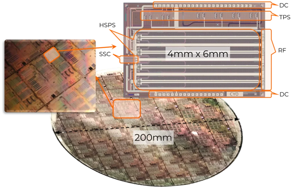
Recent demonstrations in silicon photonics have established ferroelectric Barium Titanate (BTO) as a leading electro‑optic material for next‑generation optical interconnects. Results including net 1.6 Tb/s DR4 IMDD transmission and net 1 Tb/s/λ coherent and coherent‑lite links highlight the maturity of BTO when integrated into 200 mm silicon photonics platforms, with stable operation up to 85 °C and compatibility with CMOS‑class manufacturing flows.
Barium Titanate DP-IQM Enabling Net 1 Tbps/λ ZR and Coherent-Lite Data Center Networks
A common thread across these advances is the reliance on high‑quality epitaxial metal oxide thin films, grown with precise control over crystallinity, stoichiometry, and interfaces.
Role of Metal Oxide MBE in BTO‑Enabled Photonics
In recently reported works by Industry partners (Lumiphase AG, PsiQuantum, LaLuce Cristallina), BTO thin films are formed via epitaxial growth followed by wafer‑scale integration into silicon photonics processes, enabling:
- Large Pockels coefficients for low‑voltage, high‑bandwidth modulation
- Uniform device performance across multi‑channel PICs
- Demonstrated scalability to 300 mm wafers, a key requirement for volume manufacturing
Such characteristics are fundamentally dependent on metal oxide molecular beam epitaxy (MBE), which provides atomically controlled growth conditions that alternative techniques struggle to match—particularly for complex oxides and ferroelectrics.
Find out why BTO is the optimal material for integrated Photonic Platforms and Quantum Devices.
Lumiphase as a Case Study
The Lumiphase‑enabled devices reported in these studies demonstrate what becomes possible when oxide epitaxy is aligned with semiconductor manufacturing needs:
These results underscore a broader transition: oxide electronics and photonics are no longer limited by materials physics, but by the scalability of epitaxial growth and system integration.
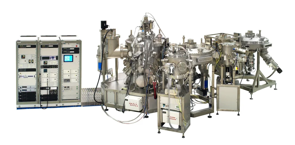
DCA’s Metal Oxide MBE Approach
DCA’s Metal Oxide MBE systems are designed specifically to address this transition by combining:
- Support for up to 12” (300 mm) wafers
- Fully automated wafer transfer
- EFEM‑based architectures compatible with silicon fabs
- Process stability suitable for high‑volume production
This architecture enables the same epitaxial platform to support quantum heterostructures, low‑dimensional oxide systems, and photonic device materials, aligning metal oxide innovation with semiconductor manufacturing workflows.
Broader Implications for Quantum and Photonic Technologies
Beyond photonics, the same MBE capabilities are essential for quantum wells, wires, dots, and correlated oxide systems, where interface perfection and reproducibility are decisive. As demonstrated by BTO‑based silicon photonics, scalable oxide epitaxy is emerging as a key enabling infrastructure technology for quantum, photonic, and nanoelectronic platforms.
Conclusion
The recent Lumiphase‑enabled demonstrations provide a clear example of how metal oxide MBE has evolved from a research tool into a manufacturing enabler. Systems that deliver atomic precision, automation, and fab compatibility are now central to translating oxide materials from the laboratory into deployed technologies.
Metal Oxide MBE – engineered for discovery, proven for production.
Data Courtesy of Lumiphase AG, Switzerland.
–
Achivements at a glance:
- Barium Titanate ((BaTiO3) or BTO) is enabling a breakthrough 1.6T (4×448 Gbps PAM4) data rate, presented at the 2026 Optical Fiber Communication Conference (OFC) by McGill University, Ciena, and Lumiphase. This technology utilizes a thin-film BTO DR4 chip integrated on a commercial silicon photonics platform in the O-band, achieving high-speed data transmission with a 3 nm CMOS SerDes. [1]
–
Key highlights of this advancement:
- Performance: Achieves a net 1.6T data rate via 4×448 Gbps PAM4 signaling.
- Technology: Uses a monolithically integrated barium titanate (BTO) on a commercial silicon photonics platform.
- Application: Ideal for high-speed, compact optical data links.
- Collaboration: Developed by researchers from McGill University, Ciena Corporation, and Lumiphase AG, as presented in OFC 2026 postdeadline paper Th4B.3/4. [1, 2]
–
Links to our partners publications:
