BaTiO₃ (BTO) Growth Process Development
Barium Titanate (BTO) Wafer Development
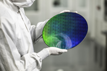
Barium Titanate (BTO) Wafer Development systems are used by industry-leading customers to develop and manufacture advanced oxide materials and substrates. One example is La Luce Cristallina, which utilizes DCA deposition technology in the development and production of high-quality Barium Titanate (BTO) wafers for research and advanced device applications.
The combination of DCA’s precise process control, excellent temperature uniformity, and flexible system architecture enables the reliable growth and optimization of complex oxide materials, supporting demanding requirements for crystal quality, reproducibility, and scalability.
This collaboration demonstrates how DCA systems help customers move from process development to the commercialization of advanced materials, creating long-term value for both research and industrial applications.
Key Facts:
Large-scale 8-inch BTO wafer manufacturing
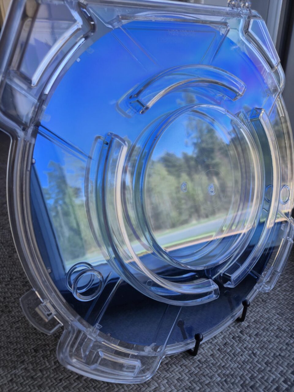
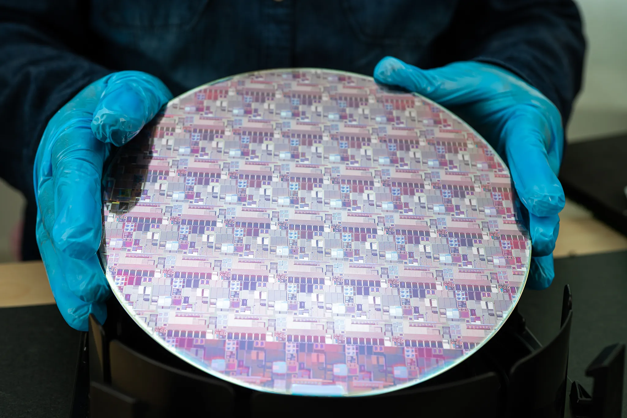
La Luce Cristallina has deployed a fully automated 8-inch wafer production platform supplied by DCA Instruments for manufacturing epitaxial Barium Titanate (BaTiO₃, BTO) and Strontium Titanate (STO) wafers on silicon and SOI substrates.
Combines MBE and UHV sputtering technologies
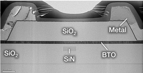
The production tool integrates an MBE chamber for STO growth and a UHV sputtering chamber for BTO deposition, enabling precise crystalline oxide integration on silicon for advanced photonic devices.
Targeted at next-generation silicon photonics
The BTO wafer platform is being developed primarily for high-performance electro-optic modulators used in optical interconnects, AI data centers, sensing, computing, and future quantum photonic applications.
Kex Benefits of the BTO Wafer Platform:
Ultra-High Electro-Optic Performance
Barium titanate provides exceptionally strong electro-optic properties, enabling faster and more efficient modulators than conventional silicon photonic approaches.
Lower Power Consumption
BTO-based modulators can operate at lower voltages, reducing power requirements for AI data-center optics and high-density optical interconnects.
CMOS and Foundry Compatibility
The wafers are designed to integrate with existing silicon manufacturing processes, allowing adoption without major fab retooling.
- Scalable High-Volume Production
The DCA Instruments automated system, together with RF sputtering technology, supports production of multiple 200-mm wafers per day, enabling commercial-scale manufacturing.
- Broad Application Potential
Beyond telecommunications, the platform supports emerging applications in quantum photonics, LiDAR, biosensing, aerospace, defense, and advanced sensing technologies.