Laser facette passivation (Comptek)
Kontrox™ Surface Engineering Technology
Transforming Semiconductor Interfaces for Next-Generation Devices
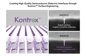
Kontrox™ is Comptek Solutions’ proprietary semiconductor surface-engineering technology developed to address one of the surface defects and native oxidation in compound semiconductors. Through advanced nanosurface engineering, Kontrox™ creates exceptionally high-quality semiconductor-dielectric interfaces, enabling improved device performance, enhanced reliability and higher manufacturing yields across a broad range of compound semiconductor materials and device architectures.
Applicable across photonics, optoelectronics and power electronics, Kontrox™ can be implemented on DCA Instruments platforms for applications ranging from sidewall passivation for microLEDs and photonic devices through to advanced dielectric interfaces and gate-stack structures for next-generation power semiconductor devices.
Applications:
- Power Electronics & RF:
Advanced passivation solutions for wide-bandgap semiconductor technologies including GaN-based power and RF devices.
- Advanced Optoelectronics:
Improved efficiency, reliability and manufacturability for emerging optoelectronic devices such as microLEDs, detectors, lasers.
- Quantum Computing:
Surface engineering solutions supporting advanced photonic and quantum device architectures.
Kontrox™ Interface Eingineering for Power & RFA
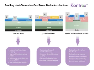
Enabling Advanced GaN Power Device Architectures
As device architectures evolve beyond conventional GaN transistors, interface quality becomes increasingly critical to electrical performance, reliability and manufacturability.
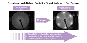
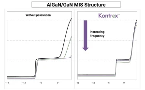
Kontrox™ enables highly stable and well-defined semiconductor-dielectric interfaces by minimizing interface defect densities and creating thermodynamically stable surface structures.
The resulting interfaces support improved electrical characteristics while enabling advanced gate-stack and MIS device architectures for next-generation power and RF electronics.
Key Advantages:
• Reduced interface trap density (Dit)
• Increased carrier mobility
• Reduced gate and surface leakage
• Enhanced dielectric-semiconductor interface quality
• Improved device reliability and long-term stability
Enabling Advanced Device Architectures
• GaN MIS-HEMTs
• p-GaN Gate HEMTs
• Vertical Trench-Gate GaN MOSFETs
• Advanced Power & RF Devices